
< Personal
> Intro
• Hardware
> Manual
> Session
— Projects: ADA, Hardware —
ADA – Analogue-Digital-Analogue Converter
The ADA-950225 is a two channel analog to digital and digital to analog converter with a resolution of 8 bit per channel and a maximum sampling rate of 38.5 kHz. It is controlled by a Z80-type processor based microcomputer. Its main use is to interface a Hewlett-Packard 3581C Selective Voltmeter / Wave Analyzer with a common two channel oscilloscope — making it to an audio frequency (AF) spectrum analyzer (SpecAn).
The computer system used is the UZE-930117#2 running on a modified version 2.01 operating system (V.2.1a). The UZE (Universal Z80 Engine) computer interfaces to a DOS based computer via a RS232C port or a Modem using a simple terminal program.
However, the ADA is self contained and does not need to be connected to a host computer. Although it was primarly built for the use described above, it can be used for other stand-alone applications, notably as a data logger running up to 10 days without intervention.
Block Diagram
The HP3581C has two analogue outputs that connect to a X-/Y-recorder. The Y-signal generates 5 Vdc for full scale, the X-signal is a ramp dc voltage from 0 to 5 Vdc from the frequency sweep. Additionally, there is a trigger input to start a sweep that can run up to 2,000 seconds and an output that lifts the pen of the recorder.
The ADA uses its external trigger output to start the sweep and the pen lift input to signal the computer, that the sweep has ended. The X-signal ramp creates the memory addresses where the sampled Y-signals are to be stored. When playing back, the memory addresses generate a fast ramp for the X-input of the oscilloscope while the memory content is used for the Y-signal. The oscilloscope must be run in the X/Y mode without timebase since the memory location generates the timebase.
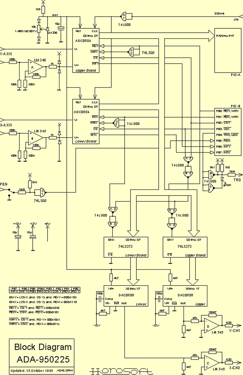
Clocking
The converter gets its primary clock from the CPU-clock which runs at 4 MHz (250 ns). All considered, a data byte is stored after approximately 1,000 CPU t-cycles, i.e. after 250 µs. The conversion rate is about 4 kHz per byte or 26 µs (38.5 kHz) for a bit.
Diagrams Converter
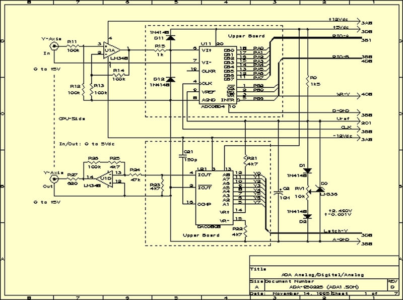
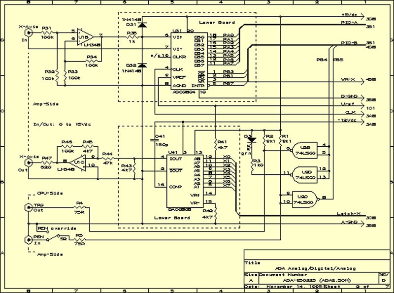
On top, the input of the Y-channel. The analogue signal is buffered by a non-inverting unity gain operational amplifier (LM348). The analog to digital converter consists of an ADC0804 whose data output interfaces to the parallel peripheral port of the CPU.
On the lower half, the data is converted to an analogue signal by a DAC0808. The output is buffered by an inverting unity gain op-amp (LM348).
At the lower right of the diagram, the reference voltage realised with a LM336 zener diode can be seen.
This is the X-channel, which is similar to the Y-channel shown above. However, here the 1 bit input and output for the external trigger and the pen lift are shown.
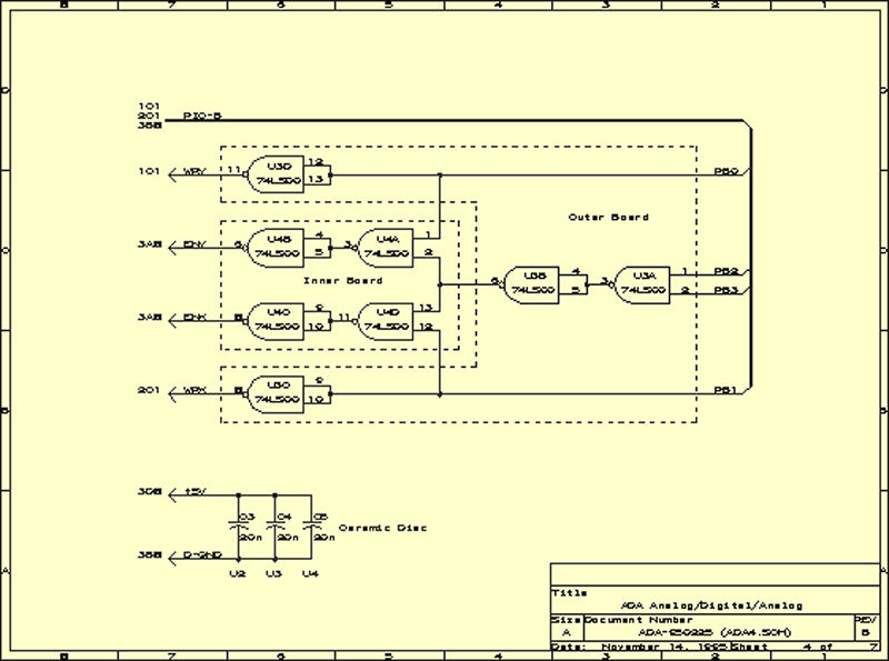
Diagrams Digital Interface
The data from the analogue to digital converter interface directly to the parallel peripheral interface (PIA) of the computer. For the digital to analogue converter, a latch must be used (74LS373).
The lower side shows the clock interface and at right the power connector as well as the RS232C interface connector for an external computer can be seen.
At the bottom, the clock conditioning circuit.
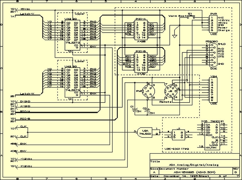
Below, the logic and control part is shown. This part generates the enable signals from the computer to the converters.
Diagrams Interface
The following diagram shows the wiring of the connectors for the RS232C and the UZE interface and the ones for the power supply. The RSC232C works a Tx- and Rx-Data line and a reduced hardware handshake using the RTS (request to send) and CTS (cleared to send) lines.
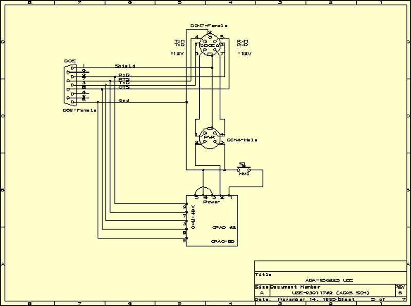
Note the push button for the non-maskable interrupt (NMI) for the Z80-type processor.
Below two interface cables. The upper one converts between the UZE connector to a 9-pin sub-D female. The lower one converts between the UZE connector to a 25-pin sub-D female. Not shown here is a small modification that connects 12 Vdc UZE pin 6 (red) via a 330 Ohm resistor to pin 20 of the sub-D 25 pin. It is used to pull-up the Modem DTR (data terminal ready). The modification was performed on 12-APR-1997.
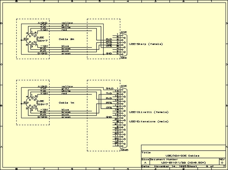
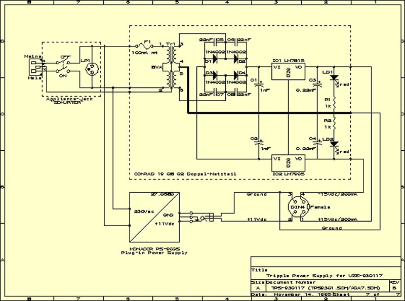
Diagram Power Supply
This diagram shows the tripple power supply. Above for +15 Vdc and -15 Vdc, below a simple raw-dc power supply that is used to create a stabilized 5 Vdc using a 7805 regulator.
ADA-950225 Pictures
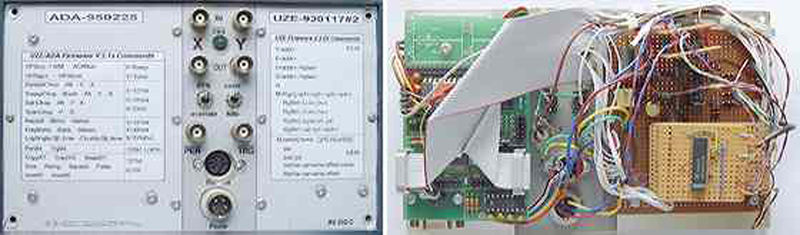
The ADA front panel with the connectors and controls. At right, the front panel from the rear side. The computer (UZE-930117#3) is on the green printed circuit board (PCB), the converter hardware on the brown breadboards. The connectors are mounted isolated on a piece of plastic cable duct (cheap and at hand).
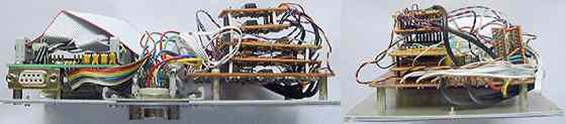
Another view of the hardware. Note the stacked breadboards for the A/D and D/A converters for each channel. This was an easy way to wire the data bus. The bottom PCB contains the control hardware for the UZE-930117#3 Z80-based computer shown at far left with the RS232C connector.
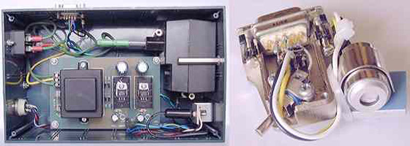
At left, the power supply. At right, a light detector built to test the logging routines. In the sub-D 9-pin male connector, a 741-type operational amplifier and a sensitivity potentiometer are mounted. ±15 Vdc come from the power supply shown at left. The light sensor was a part of an opto-isolator from a obsolete 4 GHz frequency division multiple access (FDMA) threshold extended demodulator (TED) used at the satellite earth station I worked at the time.
© 2004 - 2018 by Horo Wernli.